
Is this working? Seems like it.
We keep an internal lab blog which generally tracks our day-to-day triumphs and woes but as my time here nears its end I’d like to share these posts with a boarder audience. Mostly family and friends, but more generally those who I don’t spend everyday with. My hope is that writing for outsiders will make it clear where I’ve been missing context, and make it easier to explain to family and friends exactly what I’ve been doing here. On a more selfish note, our internal blog is also where 90% of my note-taking / ‘thinking out load’ takes place and I realized I should probably prepare a replacement for this platform.
With that said, I’ll probably forgo context in the majority of these posts and just use this as a day-to-day lab notebook as well. Due to unforeseen events (probably could of seen this coming) I’ve had a make pretty drastic change in my thesis project. So there will be a lot of experiment debugging and planning notes here in the near future. I may also move some of my more substantial posts form our lab-blog to here.
The twins
I originally named this experiment ‘twins’ for 2 reasons. Firstly, it is a copy of the previous setup I built (X88) and, second, it was going to house two identical optical cavities. The drastic change I mentioned is that this setup is now absent two optical cavities.
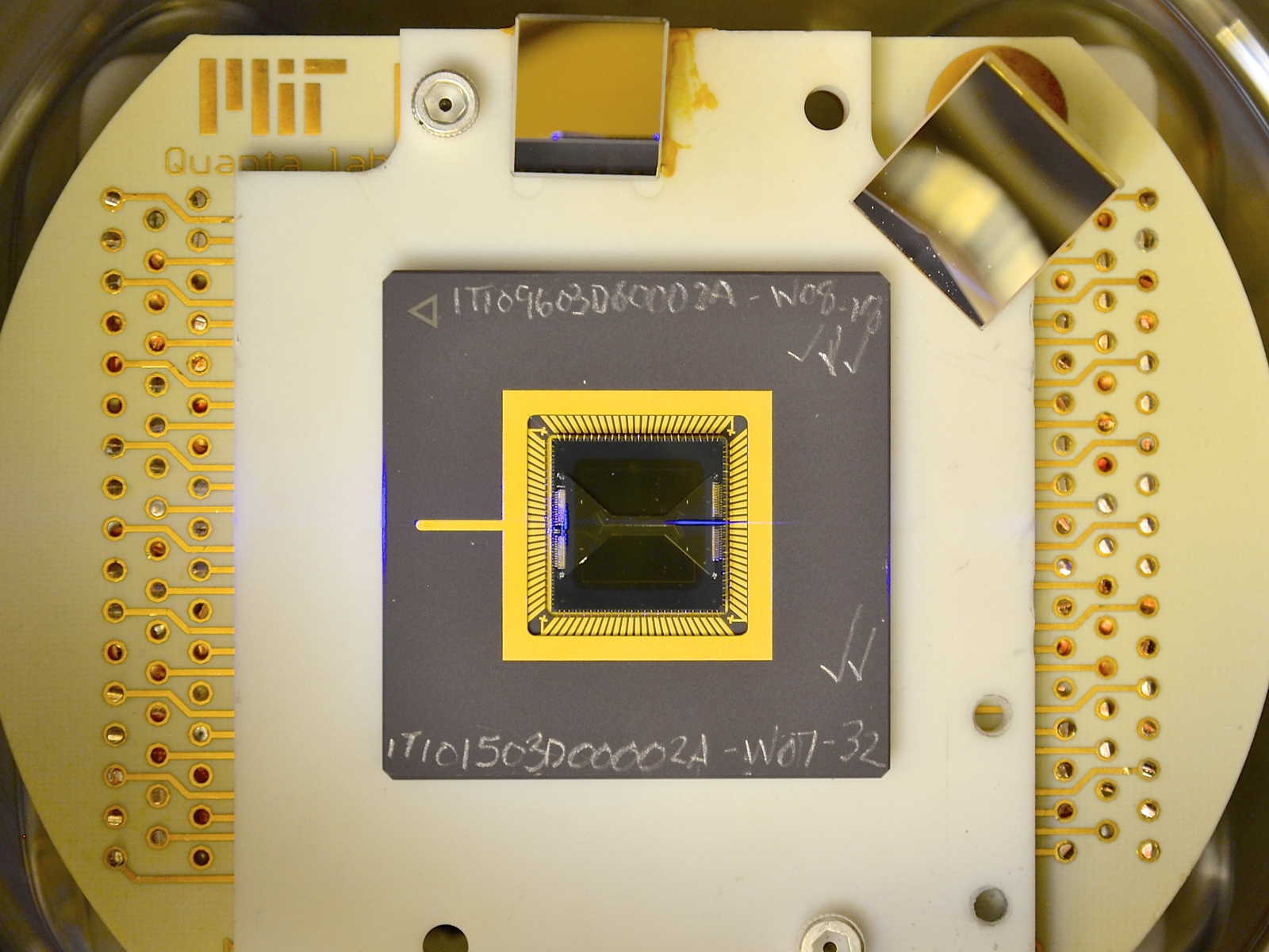
business end of Twins experiment
This is a view of the inside of our vacuum chamber, showing the installed HOA2 device along with the in-vacuum support structure. Featuring 100 electrical contacts from a vacuum feedthrough to the center cpga socket, a rear (not shown) mounted in-vacuum lens pair (f1=10mm - f2 =100mm) for imaging through the slot within the chip.
Here you can see the interesting portion of the experiment. Inside the vacuum chamber is a surface-electrode ion trap (thing at the center). Above which you can see a blue line, this is a beam of neutral atoms flowing up -> down which is being illuminated by a 461nm laser beam pointed left->right. The bow-tie looking piece at the center is the actual ion-trap portion, and you can see a number of small lines which are the electrodes used to trap and manipulate the ions. Bellow this is a purple ceramic (CPGA) which internally routes 100-electrical connections from the ion trap to its underside. Around this is a white ceramic, which is just used as a spacer / support for the pins bellow and to hold a pair of mirrors around of the ion trap. Bellow this is the main pcb (thing with the MIT logo on it) which routes the 100-connections to two db50 connectors on the vacuum flange. All of the experiments I will be talking about take place in the center bow-tie piece. Below is a zoomed in look at this chip.
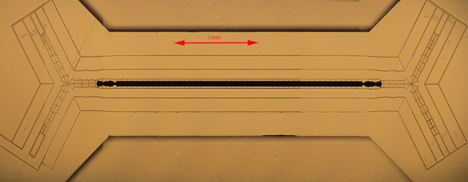
Sandia HOA V2.0 ion trap
Sandia national lab's high optical access surface electrode Paul trap. This is the device used for the majority of my thesis work.
The chip consists of 185 patterned electrodes which are routed to 96 control voltages through the CPGA. The main region of interest for our work is the central linear region, which is 4.6mm long. Of this we only look at small sections of the whole chip at a time. This is due to the magnification needed to resolve individual ions. For instance, bellow is a view of the typical reigon of interest for the experiment, along with several ions trapped in this region. The trap becomes blurry and out of focus as we focus on the ions 60micron above the trap surface (0.002in above the trap)
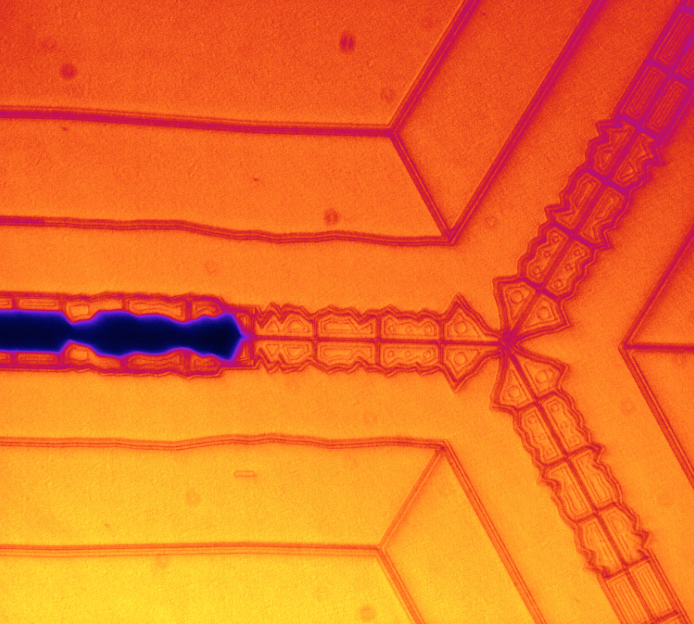
Experiment camera view
Shown is the experiment camera's view of the installed trap. Specifically looking at the loading zone focused on the trap surface, where the oven fluxed is first ionized into the trap before moving ions into the center region for experiments.
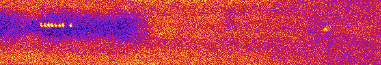
Experiment camera view ions
Experiment camera focused on ions loaded 60micron above the traps surface. The high numerical aperture used for these images leads to a very shallow depth of field resulting in an out-of-focus trap surface beneath the ions.
These images form the experiment camera are shown in false color, the actual photos are black and white, which is fine because we are only interested in one color of light, 422nm (purple-ish), which is the color the ions in the image are fluorescing. The image shows two groups of ions, the left most is a string 9 ions and the right group is a single ion. The ions are being laser cooled to a temperature of about 200 $\mu K$, at these temperature they form an orderly crystal which by tuning the trapping potential forms a string of ions with regular spacings. This is how we can tell the left-group is actually 9-ions and not just the 8-bright shown. The irregular gap between the last 2 ions is actually filled with a non-fluorescing ion, most likely another strontium isotope.